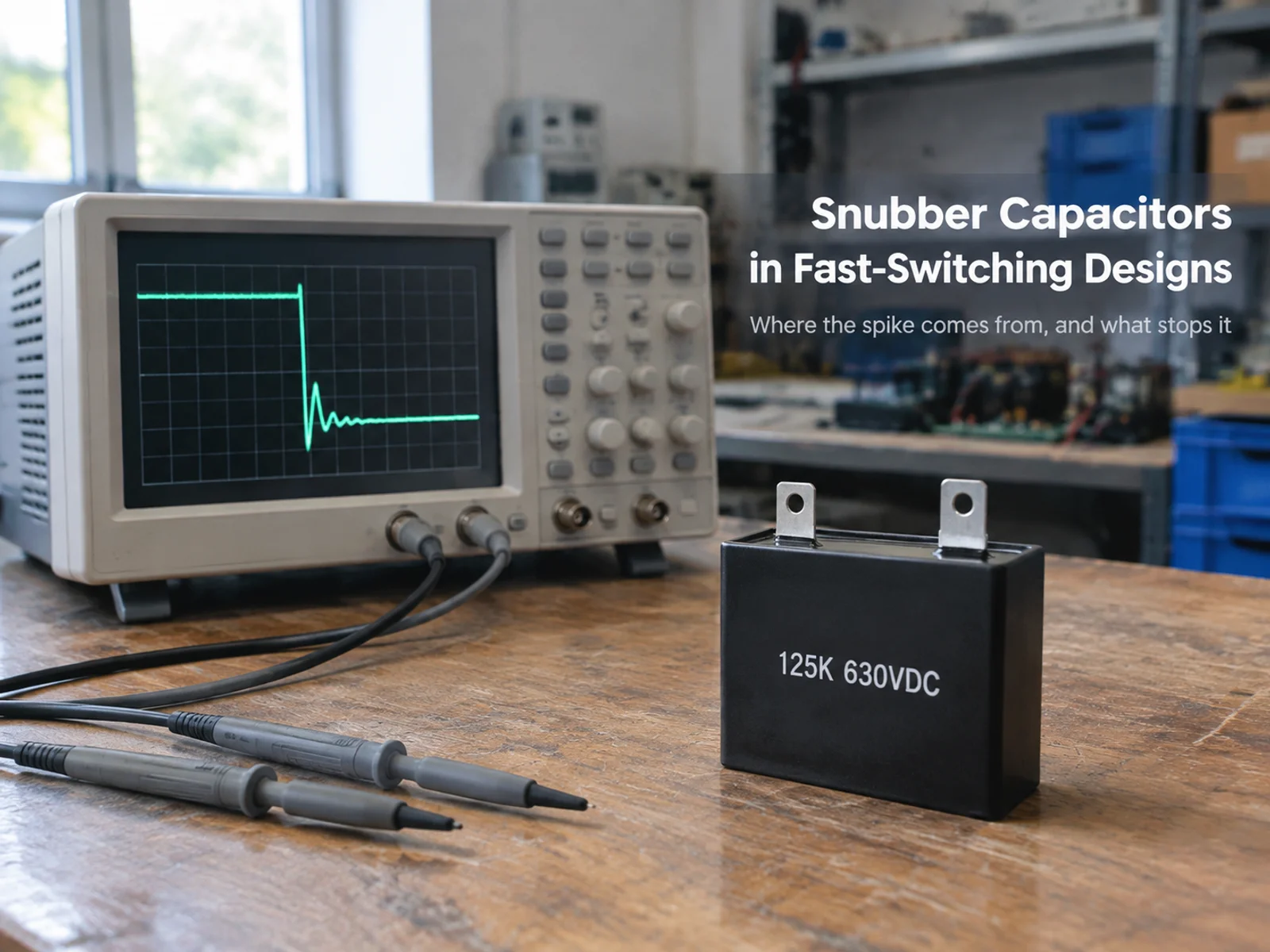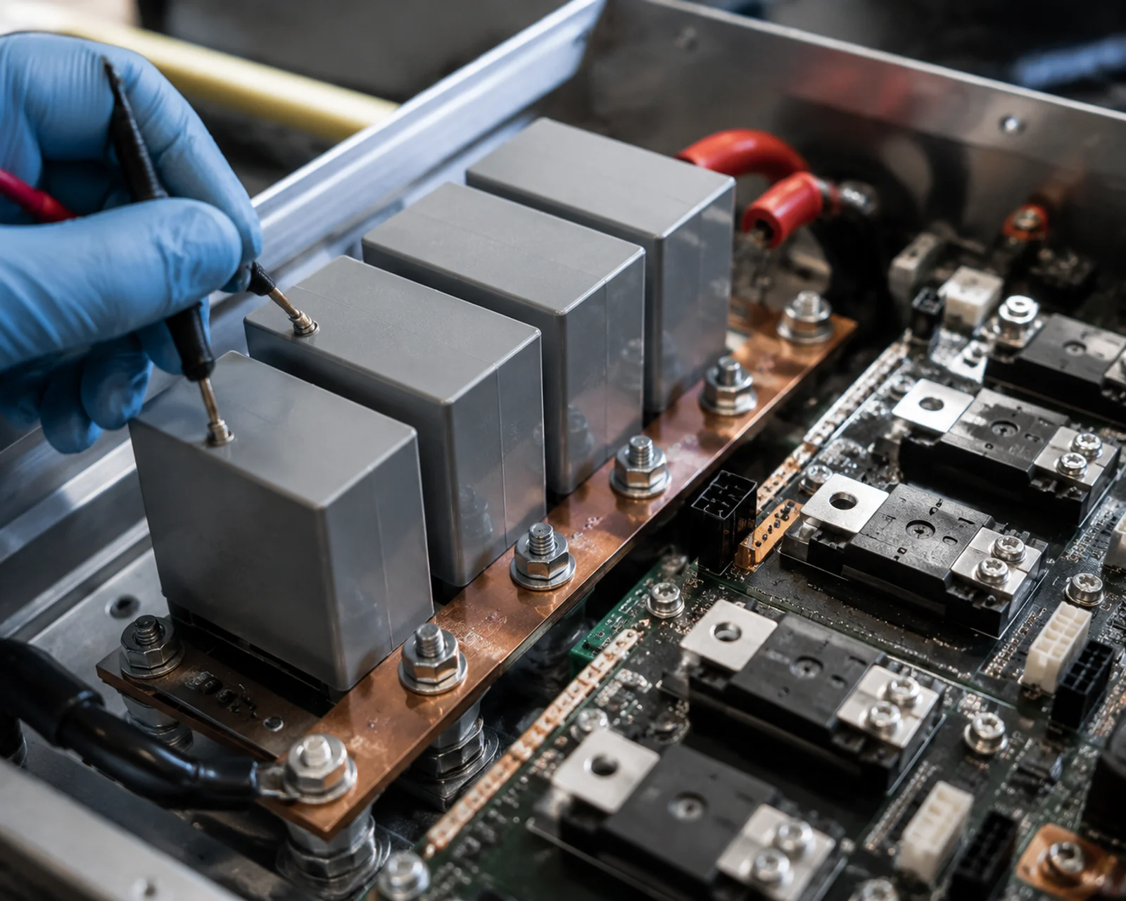
A snubber capacitor value copied from another schematic is the most common snubber on a new board. It usually arrives from a circuit that switched at a different frequency and ran at a different bus voltage. The number survives the move; the conditions that justified it do not.
This is the second article in our high-frequency power electronics series. The first covered where the spike comes from and which part answers it. What it deliberately left open was the arithmetic: how a switching edge turns into a dv/dt figure, how loop energy turns into a capacitance, and how the resistor is calculated rather than inherited.
Start From the Edge, Not From the Datasheet
A snubber capacitor’s dv/dt rating is a limit, not a target, and the number that matters is the one the circuit will actually present. The switching edge gives the capacitor two numbers to survive, and both can be worked out before a part is chosen.
Speed is the easier of the two to picture. Take the voltage the switch has to block and divide it by the time the transition takes. A silicon IGBT turning off in 200 ns across 800 V produces around 4 V/ns. A silicon carbide MOSFET in the same position can complete the same transition in 20 ns, which is 40 V/ns. Nothing about the capacitor changed between those two cases, but the demand on it changed by a factor of ten.
The peak current the capacitor must carry follows straight from that speed:
Ipeak = C × dv/dt
Put numbers into that and the reason snubber capacitors are specified by current rather than by capacitance becomes obvious. A 2.2 nF part facing 40 V/ns sees about 88 A of instantaneous current, in a package the size of a fingernail. This is where equivalent series inductance stops being a datasheet detail. An ESL of a few nanohenries is enough to oppose that current at these edge rates, and a part that blocks its own current behaves as though it were not fitted at all.
Read both figures side by side when selecting a part: the dv/dt the circuit presents, written in volts per microsecond so it can be compared with a manufacturer’s rating, and the peak current from the formula above. Both have to sit inside the part’s ratings with margin left for temperature and repeated stress. How those limits behave once they are repeated a few hundred thousand times a day is set out in our analysis of capacitor current capability and dv/dt performance.
Turn Loop Energy Into a Capacitance Value
The capacitance is set by the energy the commutation loop has to shed, and by how much voltage rise the device can still absorb.
The energy in the loop at turn-off is:
E = ½ × Lloop × I²
Without a snubber, that energy charges the device’s own output capacitance and the loop stray capacitance, and the resulting voltage rise is:
ΔV = I × √(Lloop / Cstray)
Adding capacitance in parallel with the switch lowers that rise, because the same energy now charges a larger total capacitance.
Worked example: an 800 V half bridge
A half bridge running from an 800 V bus with silicon carbide devices, switching 40 A, in a layout with 60 nH of loop inductance and 1 nF of effective stray capacitance at the switch node. The devices are rated 1200 V, and the design keeps the peak below 1000 V, which leaves 200 V for overshoot.
Without a snubber, the rise is 40 × √(60 / 1) = around 310 V, for a peak of 1110 V. That is above the limit the design allows, and it is the calculation that justifies a snubber rather than a hunch about waveform quality.
The capacitance needed to hold the rise at 200 V comes from the same relation solved the other way:
Ctotal ≥ Lloop × (I / ΔV)²
Inserting the numbers: 60 nH × (40 / 200)² = 2.4 nF as the total capacitance that has to sit at the node. The switch already contributes 1 nF of that, so the snubber itself comes out at 1.4 nF, and the nearest standard value above it is 1.5 nF.
That figure is a floor, so rounding up to the next standard value is normal. It also assumes the loop inductance is known, which is why a measured value from the real layout beats one borrowed from a similar design.
Calculate the Resistor From the Loop Impedance
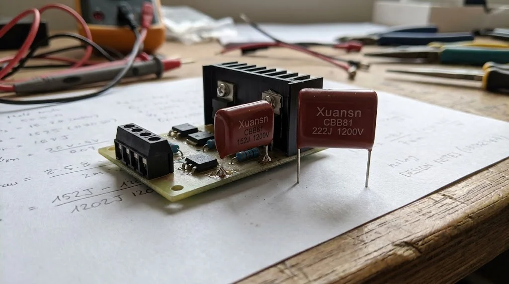
The resistor is what turns a ring into a decay. Its starting value comes from the characteristic impedance of the loop and the capacitance now sitting in it:
Z = √(Lloop / Ctotal)
For the example above, 60 nH against 2.4 nF gives roughly 5 Ω. That is a starting point, not an answer. The working range is usually a factor of two either side of it, and the two ends fail in different ways.
Go too low and the resistor stops limiting anything. The snubber capacitor discharges through it into the switch on every transition, and the current spike that produces can be worse than the ring it replaced. Go too high and the ring is still there, just lower in amplitude and easier to miss on a scope that is being read quickly. The useful test is to change the resistor in steps and watch the settling, not the peak.
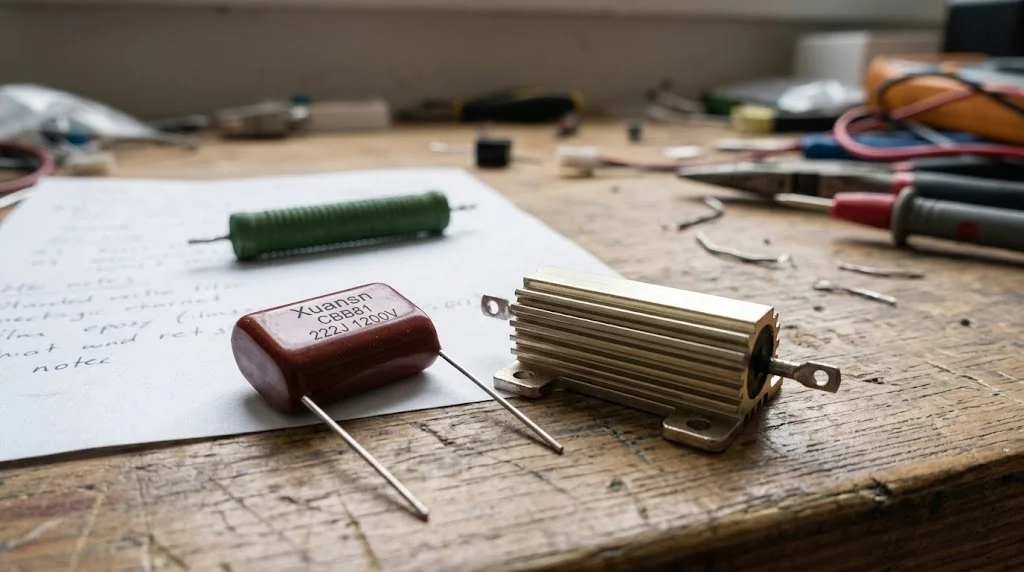
A wirewound resistor is the wrong part here for the same reason an electrolytic capacitor is wrong in the snubber position. Its inductance rises with frequency, which is precisely the quantity the resistor exists to oppose. Non-inductive film or bulk-metal types keep their resistance across the band that matters.
The Loss the Resistor Has to Carry
Every transition moves energy through the resistor, and the power it dissipates scales with both the capacitance and the switching frequency:
P ≈ ½ × Csnubber × (Vpeak² − Vbus²) × fsw
For the example, with 2.2 nF, a 1000 V peak on an 800 V bus and 20 kHz switching, the dissipation lands near 8 W. A 2 W part in that position fails in a way that looks like a snubber problem rather than a resistor problem, because its resistance drifts upward as it heats, and the damping quietly disappears.
This is the cost of the RC arrangement, and it is the reason the value deserves a calculation instead of a copy. The same capacitance on a board switching at 20 kHz with an IGBT was a comfortable 2 W problem two years ago. Raise the frequency and the identical part becomes the hottest component on the board.
Check the Values on the Bench
The calculations set the starting point. The layout decides the final value, and it does so in ways no calculator can see.
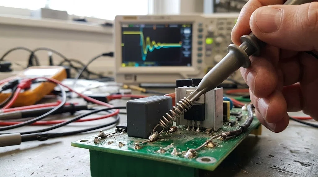
Measure the switch voltage with a probe whose ground lead is short, ideally the spring tip direct on the device. A long ground lead picks up the very loop inductance being investigated, and the waveform it produces is partly the measurement. Compare the peak with the limit the design set, then sweep the resistor upward in steps and watch two things: how quickly the ring settles, and how warm the resistor gets.
A useful confirmation is to measure the ring frequency before and after. Without a snubber, the frequency follows 1/(2π√(L·C)), and the change after fitting one tells you what capacitance actually landed in the loop. If the frequency barely moves, the snubber capacitor is not carrying current, and the likely cause is ESL or a return path that does not follow the layout on the drawing.
When the Layout Deserves the Effort Instead
A snubber cleans up what remains after the layout has been made as tight as the mechanical design allows. It does not substitute for a commutation loop that was never minimised. Loop inductance raises the energy the snubber has to absorb, so a poor layout makes the snubber larger, hotter and more expensive. It also puts more inductance in series with the snubber itself, which is the failure mode described above.
Where the loop can be tightened, tightening it is free and permanent. Where it cannot, because the busbar has to reach a module or the mechanical envelope is fixed, the snubber is the right tool and the calculation above is what keeps it honest.
What Comes After the Values
Everything above assumes the capacitor can take the stress. Whether a particular part can is a separate question, decided by its dv/dt rating and by the energy it clears per event rather than by its capacitance. That question is where the series goes next.
Questions About Snubber Values
Can I work out the snubber capacitance from datasheets alone?
Not reliably. The calculation needs the loop inductance, and no datasheet contains it. The switch package, the busbar or trace geometry and the capacitor’s own ESL all contribute, and the total is a property of the assembled layout. Estimate it for an early design, then replace the estimate with a measurement before finalising the capacitor value.
Why does the resistor need a larger rating than the calculation suggests?
Because the calculation gives an average, and the resistor sees the peak. The power formula above assumes steady-state operation at one frequency and one bus voltage. Real duty includes start-up transients, load steps and thermal derating inside an enclosure. Doubling the calculated dissipation is a reasonable starting margin, and measuring the case temperature after an hour of operation is the only confirmation that matters.
Does the resistor value matter as much as the capacitance?
It does, and it is the value most often copied without thought. The capacitance sets how far the voltage rises; the resistor decides whether the resulting ring decays or merely changes shape. A snubber with the right capacitor and the wrong resistor can leave the peak almost untouched while adding loss to every switching cycle.
What changes if I use a ceramic capacitor instead of film?
Class I ceramics work for small, low-energy snubbers and hold their value well, but their capacitance range is limited and above a few nanofarads at a few hundred volts they stop being practical. Class II ceramics are the trap: their capacitance falls with applied voltage, so a value calculated from the nominal figure can deliver far less capacitance at the voltage where it is needed, and the snubber underperforms for a reason that never appears on a bench test at low voltage.
If you are working through these numbers on a real design, send us the bus voltage, the current at turn-off, the loop inductance you are working with and the switching frequency. Xuansn manufactures metallized film capacitors for snubber duty, including the CBB81 snubber series, and our engineers will come back with a capacitance value, a dv/dt rating and a suggested part for the position. Our guide to film capacitor types covers the construction differences behind those ratings.
✉ coco@xuanxcapacitors.com | ☎ +86-769-8166 8821 | Send your specification