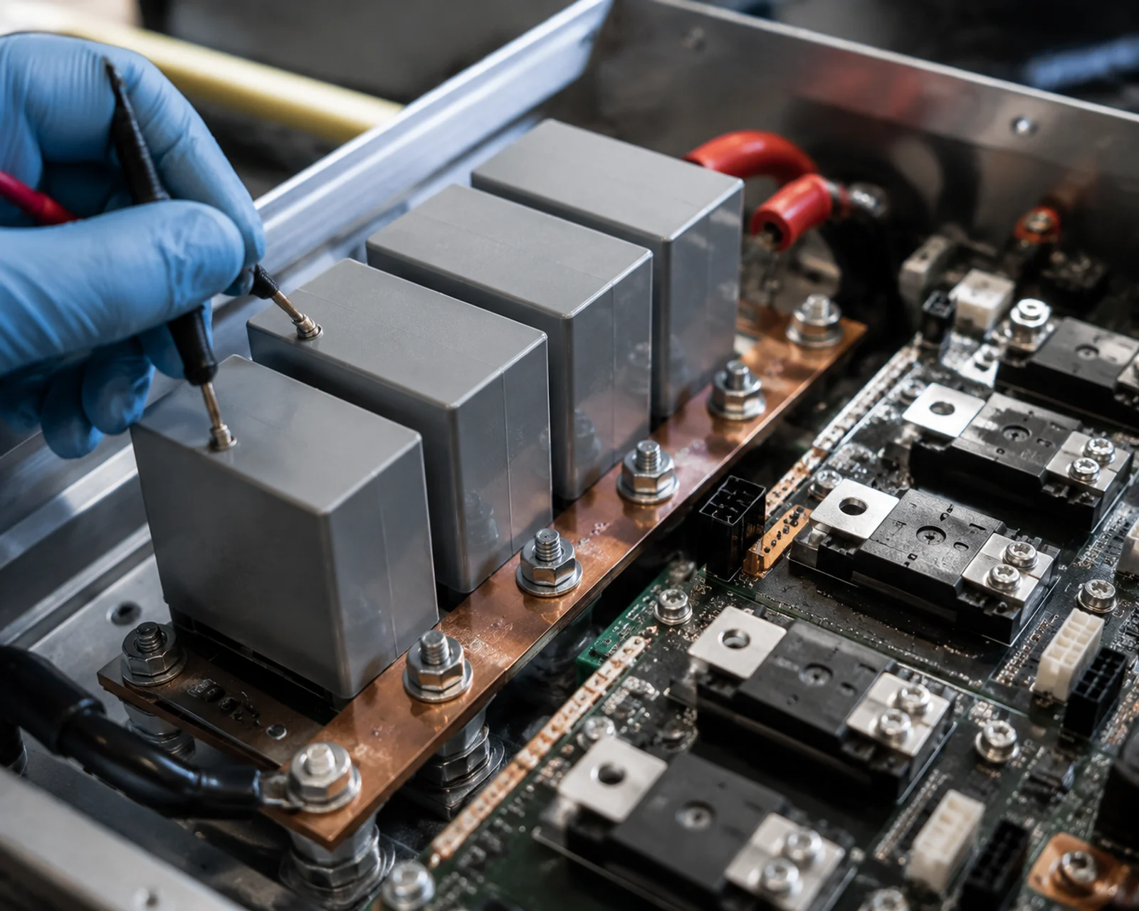
Every switching transition pushes current through the loop between the switch and its decoupling path. That loop has inductance, and inductance turns a change in current into a voltage: V = L × di/dt. The faster the switch, the larger the spike. Wide-bandgap devices switch faster than silicon IGBTs, which is why a snubber capacitor that was optional on an older design can now decide whether a circuit keeps its voltage margin or loses a device.
This article opens a series on high-frequency power electronics. It starts with the mechanism, because the mechanism decides the part. A snubber is a different kind of circuit from a filter, and the capacitor that fills the position is chosen for different parameters.
The Spike Is Built by Inductance, Not by the Switch
The device gets blamed for the overshoot. It only sets the speed. What converts that speed into a damaging voltage is the parasitic inductance in the commutation loop: the switch package and its internal bond wires, the busbar or trace that carries current out and back, and the capacitor’s own equivalent series inductance. Every millimetre of loop area adds inductance, and every nanohenry multiplies against the current slope.
A silicon IGBT turns off comparatively slowly. A silicon carbide MOSFET in the same socket can switch several times faster. The loop inductance has not changed. The voltage across it has, roughly in proportion.
Two things make this harder to live with than it was five years ago. The voltage margin has thinned: a 1200 V device on an 800 V bus has less headroom than a 600 V device on a 400 V bus, and the wide-bandgap device is the one being asked to run at the higher bus voltage. At the same time, the layouts that reduce inductance also concentrate current into less copper. The spike grows while the space available to absorb it shrinks. The DC-link side of that shift is covered in selecting film capacitors for 800 V SiC inverters; this series deals with the switching node instead.
What a Snubber Does With the Energy
A snubber gives the high-frequency current a shorter path. Instead of letting the energy in the stray inductance ring against the switch’s output capacitance, it puts a capacitor close to the device so the fast current has somewhere local to go. What happens to that energy afterwards is what separates the three arrangements most designers build.
| Arrangement | Built from | Where the energy goes | Fits when |
|---|---|---|---|
| C snubber | One capacitor across the device | Oscillates with the loop inductance, damped only by circuit losses | Ring frequency needs lowering and the resulting loss is tolerable |
| RC snubber | Capacitor in series with a resistor | Dissipated in the resistor on every transition | Ringing must be damped and heat can be managed |
| RCD clamp | Capacitor, diode and resistor | Captured in the capacitor, then bled off slowly through the resistor | Stored energy is large enough that clamping beats damping |
The choice is not about which one is better. A C snubber is cheap and adds no loss of its own, but it moves the ring to a lower frequency rather than removing it. An RC snubber actually damps the ring, and pays for it with heat that scales with switching frequency. An RCD clamp handles more energy than either, at the cost of a diode and a slower recovery of the capacitor voltage.
Why an Ordinary Capacitor Fails Here
A snubber capacitor is asked to deliver a large current in nanoseconds. At that timescale, equivalent series inductance matters more than capacitance. A part with the right microfarads and the wrong ESL will let the spike through, because the inductance blocks the very current the snubber was added to carry. This is the most common reason a snubber measures as though it were not there.
Film capacitors hold this position for a structural reason. A metallized film part in a flat case brings the electrodes out to terminals that are physically close to each other, which keeps loop area small and ESL low. The metallization also self-heals: a local breakdown vaporizes the electrode around the fault instead of shorting the part, provided the energy available is below what the film can clear.
The format also survives the dv/dt. A snubber capacitor sees the same fast voltage edge that stresses the switch, and polypropylene film handles repeated high dv/dt without the capacitance drift that Class II ceramics show under voltage and temperature. Where the pulse energy is modest and the capacitance small, a ceramic part with a suitable dielectric can work, but the film part is the default for snubber duty above a few hundred volts and above a few nanofarads, which is where ceramics stop being practical.
| Family | ESL | Capacitance range | Verdict for snubber duty |
|---|---|---|---|
| Metallized film | Low, set by case and terminal geometry | Nanofarads to microfarads | The default choice |
| Ceramic (Class I) | Very low | Picofarads to tens of nanofarads | Works for small, low-energy snubbers |
| Ceramic (Class II) | Very low | Higher than Class I | Capacitance shifts with voltage and temperature; check the derating curve |
| Aluminum electrolytic | High | Microfarads and up | Wrong tool: inductance and dv/dt limits defeat the purpose |
Matching the Snubber Capacitor to Its Position
Where the snubber sits decides what it has to survive. A capacitor across a bridge leg sees a fast edge on every switching cycle and has to hold its value over millions of them. A snubber across a rectifier sees the reverse recovery of the diode instead. The energy per event and the repetition rate are different, and they drive different parts of the specification.
| Position | What the capacitor sees | Priority in the specification |
|---|---|---|
| Across a bridge leg | A fast edge every switching cycle, high repetition rate | dv/dt rating, then ESL, then loss per event |
| Across a rectifier or freewheel diode | Reverse recovery energy, lower repetition rate | Peak current and dv/dt, then capacitance value |
| Transformer primary clamp | Leakage energy per cycle, often the largest of the three | Energy per pulse and capacitance stability |
| Across a low-voltage rail switch | Small capacitance, very high frequency | ESL above everything else |
What Goes Wrong on the Bench
Snubber problems tend to appear in the same four places, and none of them are visible on the capacitor’s datasheet.
The most common is a capacitor mounted a centimetre or two from the device. At that distance the part has already given back the inductance it was chosen to avoid, because the leads to it and back are part of the loop. A snubber only works when it sits at the terminals, with the return path as short as the outgoing one.
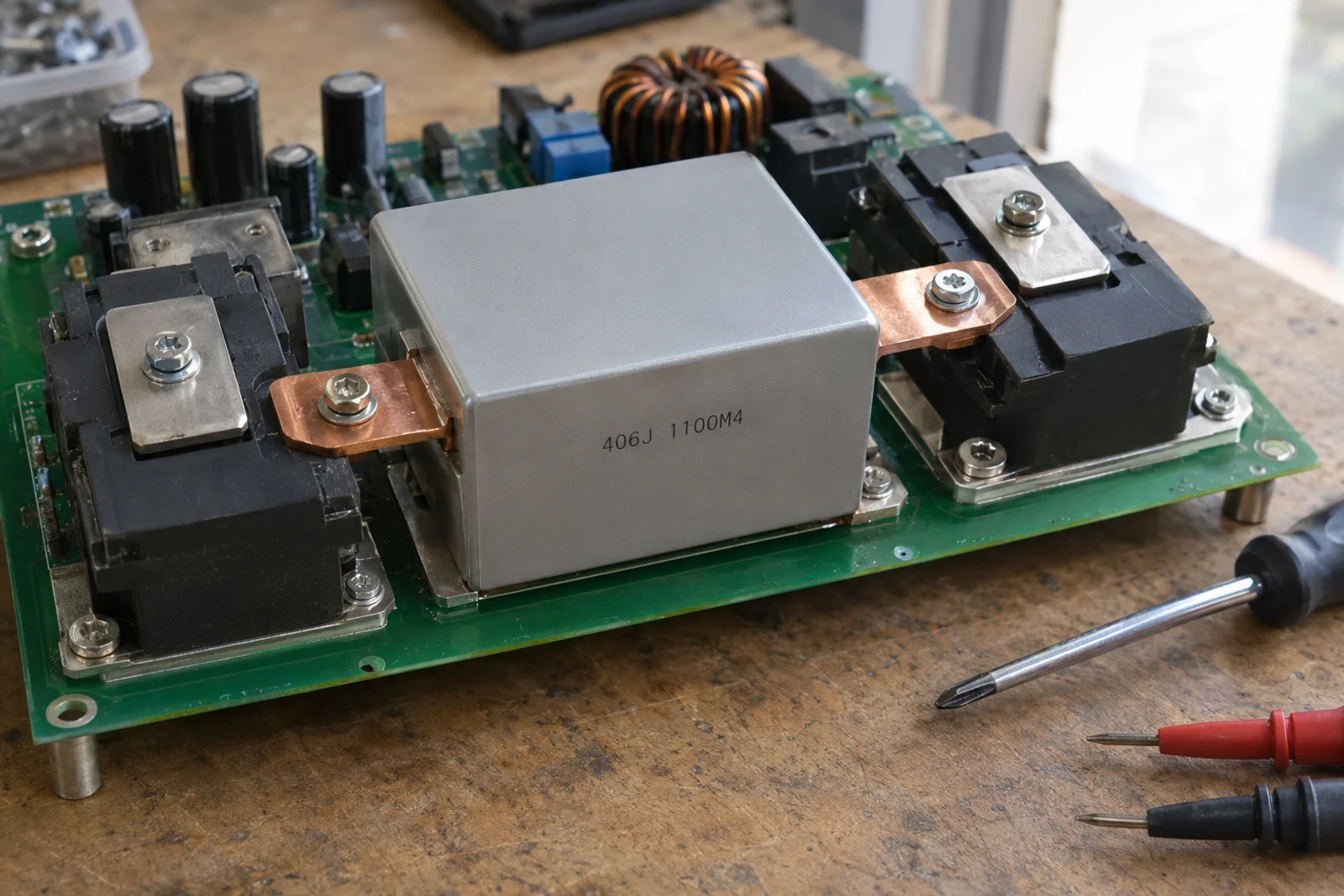
Then there is the dv/dt rating nobody checked. The snubber capacitor sees the fast edge directly, and a film part chosen for capacitance and voltage but not for dv/dt will lose capacitance as the metallization degrades. That failure is quiet. The spike creeps up over months instead of appearing as a hard fault, which is why it usually turns up on a returned unit rather than in the lab.
Resistor values get copied from older schematics more often than they get calculated. In an RC snubber the resistor sets both the damping and the loss. Too low and the snubber pulls a large current spike out of the switch on every cycle. Too high and the ring is barely touched. If the switching frequency has changed since that schematic was drawn, the old value no longer applies to it.
Last is heat with nowhere to go. Loss in an RC snubber scales with switching frequency, which is exactly the parameter that went up when the design moved to wide-bandgap devices. A snubber that ran cool on an IGBT design can end up the hottest part on the board after the switch to silicon carbide.
Where This Series Goes
Everything above is about whether a snubber works. None of it answers the other question, which is what value goes in the position. The mechanism says a snubber is needed; the numbers decide whether it does anything. That is where the next article in the series picks up: reading a dv/dt rating against an actual edge, sizing capacitance from the energy the loop must absorb, and calculating the RC resistor rather than copying one.
Common Questions About Snubber Capacitors
Can I use a ceramic capacitor instead of film in a snubber?
For small, low-energy snubbers at modest voltages, yes, and a Class I ceramic is often the better part because its capacitance does not move with voltage or temperature. The limit is practical: above a few nanofarads of capacitance and a few hundred volts, ceramic parts become large, expensive or simply unavailable, and film takes over.
Why does my snubber resistor run hot?
Because it is doing its job. An RC snubber removes energy from the loop on every transition, and the resistor is where that energy becomes heat. The dissipation scales with both the capacitance and the switching frequency, so a design that increased its switching frequency needs the loss recalculated even if nothing else changed.
What size capacitor do I need for a snubber?
Size it from the energy the loop has to absorb, not from the capacitance values you see in other designs. The stored energy in the stray inductance depends on the current at turn-off and the loop inductance. The snubber capacitance is then chosen so the resulting voltage rise stays inside the margin the device has left. Calculation first, then verification on the bench with the actual layout.
Does a snubber replace good layout?
No, and treating it that way is how designs end up with a snubber that cannot do its job. Reducing loop area is still the primary move, and it is free. The snubber cleans up what is left after the layout has been made as tight as the mechanical design allows.
Xuansn manufactures metallized film capacitors for snubber and high-frequency power duty, including the CBB81 series used across bridge legs and rectifier positions. If you send the switching frequency, the current at turn-off and the loop inductance you expect, we will come back with a capacitance value, a dv/dt rating and a part number. Reach us at coco@xuanxcapacitors.com.