You can size a snubber capacitor and resistor perfectly, check their ratings, and still watch your switches destroy themselves during transients. The part is rarely at fault. What fails is the route that carries the snubber current to the switch. Once that route adds more inductance than the damping can absorb, the snubber branch stops behaving like a resistor at the frequency that matters and starts behaving like an inductor, and the damping you paid for quietly disappears.
Low inductance is the assumption underneath every fast-switching design, and it is the one assumption nobody draws on the schematic. When you sized the snubber you would have focused on the capacitance that absorbs the charge and the resistance that damps the oscillation. On the bench, a snubber is a loop: wire, trace, busbar, and the two parts sitting inside it. Widen that loop and the inductance it adds decouples the capacitor from the switch, which makes the earlier numbers irrelevant at the moment they are needed.
What decides whether the snubber works is the space between the switch terminal and the capacitor case, and that space is where most designs quietly lose the argument.
The Capacitor You Sized Is Only Half a Circuit
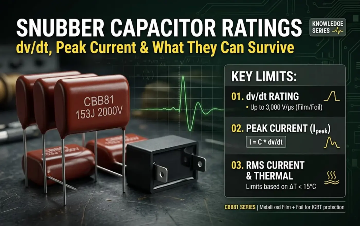
The standard design approach focuses on component ratings. You calculate the required capacitance to handle the energy of the spike, select a resistor to dissipate it, and inspect snubber capacitor ratings to ensure the parts can survive the dv/dt and pulse currents. However, that paper circuit assumes a mathematically perfect connection. In the real world, the physical route from the switch terminal, through the snubber resistor, into the capacitor, and back to the return node is an inductive path.
If you have been following this series, you already know where the voltage spike comes from, which is the product of stray inductance and the extremely fast di/dt during a turn-off event. Treating the snubber as an isolated patch that can be wired anywhere convenient on the chassis is the most common way to lose it. Sizing the capacitor is only half the design process; the other half is managing the interconnect inductance. Let the connection inductance run high and the branch is effectively disconnected from the switch at the very frequency you need to suppress.
The Snubber Has Its Own Loop, and It Is Not Small
Two different inductances are in play, and mixing them up is why this section exists. The commutation loop is the one that creates the spike in the first place, and it belongs to the inverter layout. The connection inductance is the loop you create by bolting the snubber onto the switch. They are separate quantities, they are added in separate places, and the rest of this article is about the second one.
Inductance is not determined by wire length alone. It is a function of loop area. The larger the physical space enclosed by the outgoing and return paths of a circuit, the more magnetic flux it can capture and the higher its inductance will be. Flying leads that take a circuitous route to reach a capacitor create a massive loop, even if the conductor itself is short.
As a rule of thumb, a single wire running through space with a distant return path exhibits approximately 1 nH of inductance per millimeter of length. This means a seemingly short 25 mm lead wire, combined with a 25 mm return connection, can easily add 50 nH to the circuit. For comparison, a typical snubber film capacitor might have an internal equivalent series inductance (ESL) of only 5 to 10 nH. In a typical installation the wiring carries most of the inductance in the snubber branch, far more than the part contributes internally.
To lower this value the outgoing and return conductors have to be coupled. Run them alongside each other, pressed flat against a grounded busbar, or twisted together and the figure drops to roughly 0.5 nH/mm. Laminated busbars and closely spaced ground planes go lower still.
| Wiring Method | Estimated Inductance (Rule of Thumb) | Equivalent Distance to Hit 60 nH Budget |
|---|---|---|
| Single conductor, distant return | ~ 1 nH / mm | ~ 60 mm total length |
| Twisted pair / tightly pressed conductors | ~ 0.5 nH / mm | ~ 120 mm total length |
| Laminated busbar / Ground plane sandwich | Significantly lower | Far exceeds typical mounting lengths |
Doing the Budget With Known Numbers
To see how this inductance degrades performance, let us carry over the benchmark system from our guide on calculating the snubber capacitor and resistor. In that 800 V / 40 A design, the commutation loop inductance was 60 nH, the switch node stray capacitance (Cstray) was 1 nF, and the allowable overshoot was 200 V, giving a 1000 V peak on a 1200 V device. This generated an unsnubbed ringing frequency (fring) of 20.55 MHz.
The design required a 1.4 nF snubber capacitor (selected at 1.5 nF, bringing the total capacitance Ctotal to 2.4 nF) and a 5 Ω damping resistor. When installed correctly, this network shifts the ringing frequency down to 13.26 MHz. At this frequency, the angular frequency (ω) is 8.33 × 10⁷ rad/s.
For a snubber to actually provide damping, the connection’s inductive reactance must not choke off the resistive path. Specifically, the reactance of the connection inductance (XL = ωLs) must be significantly lower than the snubber’s damping resistance (R). Our ceiling for the connection inductance is the point where XL equals R:
Ls ≤ R / ω = 5 Ω / 8.33 × 10⁷ rad/s = 60 nH
This 60 nH is the connection inductance budget. It includes the capacitor’s internal ESL, the resistor’s parasitics, and the physical trace, busbar, or wire loop connecting them to the switch. A simple wire pair allowed to drift apart spends the whole 60 nH budget inside 60 mm of total lead length. Splicing a snubber onto a remote board or using flying wires almost always guarantees you will exceed this budget.
| Connection Inductance (Ls) | Reactance (ωLs at 13.26 MHz) | Total Branch Impedance (Zsnub) | Self-Resonance (with 1.5 nF) | Damping Assessment |
|---|---|---|---|---|
| 5 nH | 0.4 Ω | 5.02 Ω | 58.1 MHz | Excellent; almost no damping loss |
| 20 nH | 1.7 Ω | 5.27 Ω | 29.1 MHz | Acceptable; minimal degradation |
| 60 nH | 5.0 Ω | 7.07 Ω | 16.8 MHz | Budget ceiling; borderline function |
| 100 nH | 8.3 Ω | 9.72 Ω | 13.0 MHz | Self-resonance matches ringing; failed |
| 200 nH | 16.7 Ω | 17.40 Ω | 9.2 MHz | Inductive branch; damping is gone |
Where the Damping Actually Disappears
At 200 nH of connection inductance, the branch impedance at the 13.26 MHz ring rises from 5 Ω to 17.4 Ω. The characteristic impedance of the circuit (Z0) is only 5 Ω, so a branch sitting at 17.4 Ω is no longer a bypass at all. It carries almost none of the high-frequency current, and the ring survives untouched.
An alternative way to analyze this is through self-resonance. The snubber capacitor (1.5 nF) and the connection inductance (Ls) form a series resonant tank. For the snubber to work, its self-resonant frequency must be higher than the ringing frequency of the circuit (fring).
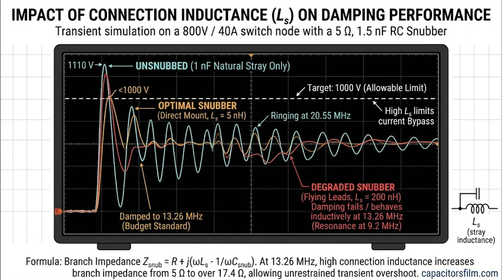
At 20 nH, the snubber’s resonant frequency is 29.1 MHz, which is comfortably above the 13.26 MHz ringing. However, if the connection inductance reaches 200 nH, the resonant frequency drops to 9.2 MHz. Since this self-resonance is now below the ringing frequency, the capacitor looks like an inductor at 13.26 MHz, and the entire damping network breaks down.
Six Snubbers in One Enclosure Do Not Share the Work
The danger of parasitic inductance is most apparent in multi-phase power assemblies, such as a three-phase bridge in a single enclosure containing six switches. Due to the physical spacing of the terminal blocks and busbars, every snubber branch will have a different connection length and, consequently, a different connection inductance.
Consider two parallel branches on the same electrical node: Branch A is mounted directly on the terminal with 20 nH of connection inductance, while Branch B is routed through 120 nH due to its physical location. At 13.26 MHz, Branch A has an impedance of 5.27 Ω, while Branch B has an impedance of 11.18 Ω.
| Parallel Branch | Connection Inductance | Impedance (at 13.26 MHz) | Current Distribution | Relative Damping Loss / Heating |
|---|---|---|---|---|
| Branch A (Directly mounted) | 20 nH | 5.27 Ω | 68% | Base loss (highest stress) |
| Branch B (Wired further away) | 120 nH | 11.18 Ω | 32% | Loss in A is 4.5 times higher |
Because the current divides inversely with impedance, Branch A absorbs 68% of the transient current while Branch B takes 32%. Resistive loss goes with the square of current, so the resistor in Branch A dissipates 4.5 times the power of the one in Branch B.
The failure pattern runs backwards from what the layout suggests. The snubber mounted with the lowest inductance, the one with the tidiest connection, runs much hotter and fails first, because it is doing almost all of the damping work. Repair teams usually read that as a bad capacitor and replace it, when the part was overloaded by the routing of its neighbour.
Typical signs of this issue on the bench or in the field include uneven temperatures across matching snubber banks, charred damping resistors, or a pattern where the same specific node repeatedly fails after replacement.
A Bench Check That Takes Ten Minutes
If you suspect connection inductance is undermining your design, you can run a quick diagnostic test using an oscilloscope without disassembling the system. Probe the switch node during turn-off and record the ringing frequency of the voltage spike with the snubber active, then temporarily disconnect the snubber capacitor and measure the unsnubbed ringing frequency again.
If the snubber is connected with low parasitic inductance, you should see a significant drop in frequency when the capacitor is introduced, typically by a factor of 1.55 (corresponding to √(Ctotal / Cstray) = √(2.4 nF / 1 nF)). At the same time, the voltage peak should be effectively clamped, falling from the 1110 V unsnubbed level to below the 1000 V target.
However, if the frequency barely shifts and the voltage spike is unchanged, the snubber branch has been choked by connection inductance. The capacitor is electrically disconnected at high frequencies, and no amount of component-level replacement will solve the issue until the mounting path is redesigned.
What Good Mounting Looks Like
To keep connection inductance within your budget, the snubber network must be tightly integrated with the power semiconductor terminals rather than wired separately on the chassis:
- Mount the capacitor directly onto the IGBT or MOSFET module terminals using lugged film housings built for it. Avoid placing the snubber on a remote PCB and running wires to the module.
- Use laminated or stacked busbar configurations where the outgoing and return paths are separated by only a thin layer of insulation to cancel out mutual inductance.
- If you must use discrete wires, run the outgoing and return paths as a tightly twisted pair or bound parallel harness to minimize the loop area.
- Keep lead wires as short and as direct as possible, avoiding point-to-point wiring and general-purpose terminal strips.
- The snubber resistor may be placed slightly further away if required to manage thermal dissipation, but the CBB81 polypropylene film capacitors and snubber networks must remain directly at the switch node.
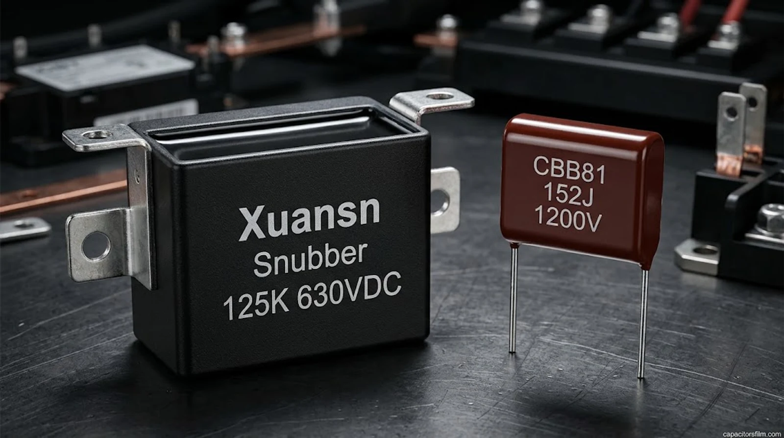
Always ensure the capacitor body is not directly subjected to excessive heat from nearby resistors or power semiconductor casing. High ambient and local temperatures can quickly push the internal hotspot beyond its limit, demanding careful thermal monitoring alongside your inductance budget.
Where This Series Ends
Four articles, one chain: how stray inductance and fast di/dt make the spike, how the RC values are calculated, which film parts survive the stress, and now how the assembly has to be built for those values to mean anything. The first three decide whether the snubber works on paper. This one decides whether it works on the board.
Common Questions About Snubber Mounting
How much inductance does a snubber connection add?
As a rule of thumb, single uncoupled wires add roughly 1 nH of inductance per millimeter of length. Splicing a snubber with 50 mm of lead wire and an equivalent return path will add about 100 nH of parasitic inductance to the branch. This is often more than ten times the internal ESL of the capacitor, which typically sits under 10 nH.
Can I mount the snubber capacitor away from the switch and run wires to it?
Only if the added inductance remains within your specific connection budget (such as 60 nH in our example). In high-frequency systems, even short wire runs can introduce enough inductance to prevent the snubber from suppressing transients, making direct terminal mounting the only viable option.
Why does one snubber in a three-phase bridge run hotter than the others?
Physical layout decides it. The snubber with the shortest connection path has the lowest branch inductance, which gives it the lowest impedance at the ring frequency, so it draws the larger share of the transient current. That share heats its resistor far more than its neighbours and wears the part out first.
Does a low-ESL capacitor fix a bad layout?
No. Upgrading to a capacitor with extremely low internal ESL will not make up for an inductive mounting loop. The parasitic inductance of a few centimeters of lead wire or poor PCB routing will completely swamp any small improvements made at the component level.
Working on a snubber layout you cannot get to behave? Send the bus voltage, the turn-off current, the commutation loop inductance you expect, the switching frequency and the physical distance between the switch and the capacitor, and Xuansn will come back with a capacitance value, a connection inductance budget and a CBB81 part number that fits. Reach us at coco@xuanxcapacitors.com, call +86-769-8166 8821, or send your specification through the contact page.