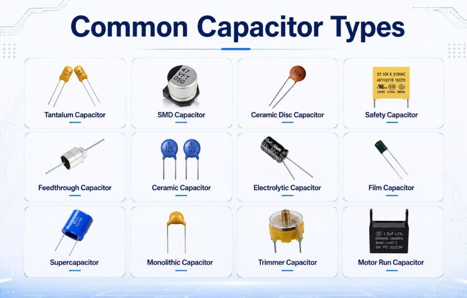
🍉Different from other chip components, use of multilayer ceramic capacitors may be damaged due to large stress due to the thin internal electrodes and dielectrics, and the dielectric is very brittle: the combination of internal electrodes and terminal electrodes of multilayer ceramic capacitors is also relatively Fragile. Therefore, relevant precautions should be observed when soldering multilayer ceramic capacitors.
1 The aging problem of the second type of ceramic dielectric capacitors
🍓X7R and Y5V media age (capacitance decay) over time. In general, the capacitance of X7R and Y5V dielectric capacitors is 99% of the initial value after passing through the Curie point (about 130°C) for 10h, and the capacitor is 99% of the initial value after 100h in the normal temperature environment, and the capacitor is the initial value after 1000h. 98% of the value: The capacitance of Y5V medium after 100h at room temperature is the initial value, after 1000h it decays to 94%, and after 10000h it decays to 88%.
🍈The method to restore the capacitance of the capacitor is relatively simple, which is to raise the temperature of the ceramic capacitor to above the Curie temperature. For example, use a soldering iron to touch and solder the pads of the multilayer ceramic capacitors for a few seconds, or place the entire circuit at 130 ℃. environment for a period of time. The former is more practical and safe, because other components are not damaged by high temperature at this time.
🍒The capacitance of X7R and Y5V dielectric ceramic capacitors decreases when a DC bias voltage is applied. In particular, the capacitance drop of Y5V dielectric ceramic capacitors is particularly obvious, and it is necessary to pay attention to the application.
2 General Precautions for Ceramic Capacitors
🍑Ceramic capacitors are fragile and abrasive substances. If handled improperly, they may cause mechanical damage to cracking or chipping. Therefore, the following aspects should be paid attention to:
2.1General handling matters needing attention
(1) Multilayer ceramic capacitors are easily broken when thrown. In addition to surface damage, capacitance changes, dissipation factor rises, insulation resistance drops, and dielectric strength drops.
(2) Rolling the bulk multilayer ceramic capacitors together will grind the metal of the terminals to the surface of the other capacitors. Metal traces left on capacitors can lead to failure hazards such as creepage.
(3)🥜Multilayer ceramic capacitors should never be handled by hand, because sweat and skin oil will make the solderability of the terminal electrodes worse, and it is difficult to clean up.
(4)🍧Multilayer ceramic capacitors are never allowed to be handled with metal tools. Metal tweezers will chip off chips or leave metal traces on the surface of the capacitor. Plastic or plastic-encapsulated metal tweezers are recommended when using tweezers. Use to keep the applied pressure to a minimum.
2.2 Matters needing attention during transportation
(1) To the extent possible, it should be shipped in its original unopened packaging. If opened, the protective material originally attached should be replaced and resealed.
(2)🍪Do not pack multilayer ceramic capacitors directly with paper or cards, because some papers contain sulfur components, which will adversely affect the solderability of the capacitors. Bulk laminated ceramic electro-pneumatics should be cushioned with foam plastic that does not contain sulfur to avoid damage caused by collision and grinding during transportation.
2.3 Use of multilayer ceramic capacitors:Storage
(1)🍦If the multilayer ceramic capacitors encounters sulfur dioxide, chlorine, other acidic gases or humid air, the electrode terminals are easily oxidized and affect the solderability.
(2)Paper and rubber contain sulfur substances and cannot be stored together with multilayer ceramic capacitors.
(3)🧁Unused multilayer ceramic capacitors should preferably be kept in their original packaging, and those that have been opened should be resealed as soon as possible. It can also be stored in an airtight container to avoid environmental impact. Therefore, some multilayer ceramic capacitors manufacturers will place multi-disc capacitors in a relatively sealed can.
(4)If it is stored for a long time, it is best to maintain it between -5 and +40 °C, and the relative humidity is between 40% and 60%.
(5)Direct sunlight will deteriorate the tape and contaminate the capacitor.
(6)🍭Stored in the above method, the original packaging can be stored for two years.
3 Use of multilayer ceramic capacitors:Mounting and Soldering
3.1 The influence of the installation position of the components on the components
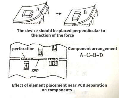
🥭Since the multilayer ceramic capacitors is easily damaged when subjected to bending force, in the PCB design, the placement position of the multilayer ceramic capacitors should pay attention to select the position where the chip is subjected to the least pressure when the PCB is bent or deflected. If the PCB is likely to be bent under force, the orientation of the components should be
🍍The direction perpendicular to the force, as shown in Figure 3.49, the placement direction of B is better than the placement direction of A. Such force will cause the least damage to the contact between the inner electrode and the outer electrode.
🥝Similarly, several or even dozens of PCBs are usually produced at the same time during PCB production. When using, each PCB needs to be separated. The separated places are usually easier to separate by perforation or gap. In this way, the different placement positions of the ceramic capacitors near the separation of the PCB, Figure 3.49 The effect of the circuit and the direction of the multilayer ceramic capacitors on the ceramic capacitor is also different when the PCB is separated.
🍅The influence of the placement position of the board on the components, as shown in Figure 3.49 below, there are four multilayer ceramic capacitors with different placement positions and orientations. The order from worst to best component placement is: A is the worst, B is slightly better, and D is the best. The reason is that when the PCB is separated, the A component is subjected to the largest force in the same direction of the component; the C component is farther away from a certain separation, so the force is smaller than that of A, but it is still subjected to the force when the PCB is separated; the position of B is in the separation. When the PCB is separated, it is a gap, so the force is better than that of C. Since the placement direction of component D is perpendicular to the force when the PCB is separated, the harmful force is the least.
3.2 Requirements for solder paste printing
🥑SMD components can be soldered to the circuit board by reflow soldering and small peak soldering, and individual components can also be manually soldered to the circuit board.
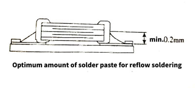
🥒The first process for reflow soldering is the printing of solder paste. Using too thick solder paste will result in too much solder. This makes the chips on the PCB more susceptible to the mechanical and thermal stress of the board, and can lead to
🌼If the chip is damaged, too little solder paste will cause insufficient bonding strength on the external electrodes, resulting in the chip falling off from the PCB. Be sure to distribute the solder paste evenly over the terminal surface with a thickness of at least 0.2mm, as shown in Figure 3.50.
3.3 Precautions when mounting SMD components
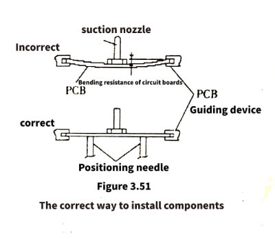
🌻When the nozzle is installed, the bottom dead center is too low, which will cause a large load on the chip, which will damage the chip, as shown in the upper picture in Figure 3.51. At this time, the bottom dead center of the nozzle can be adjusted by correcting the distortion of the PCB. Under normal circumstances , the bottom dead center of the suction nozzle must be on the upper surface of the PCB, as shown in the lower part of Figure 3.51. The nozzle pressure for chip mounting must be limited to a static load of 1 to 3N. The dust particles and dust deposited between the suction nozzle and the inner wall of the cylinder will make the suction nozzle not move smoothly, which will cause a large load on the chip during installation, resulting in damage to the chip. After the positioning claw is worn, it will exert uneven force on the chip during positioning, resulting in chip damage. The suction nozzle and positioning claw must be regularly maintained, inspected and replaced.
3.4 Reflow soldering
🌞The sudden heating of the chip will cause the chip to deform due to internal expansion and excessive internal stress, thereby damaging the chip. Therefore, during preheating, it is necessary to maintain the temperature difference ΔT within the recommended range for the components being welded. The smaller the ΔT value, the smaller the pressure on the chip. When the component is immersed in the solvent after installation, be sure to maintain the temperature difference (ΔT) between the component and the solvent within the range required by various components. The standard heating conditions and allowable time for reflow soldering are shown in Figure 3.52.
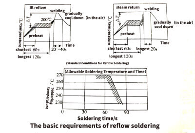
Insertion of lead components: If the PCB is bent when mounting lead components (such as transformers and ICs, etc.), the chips may be damaged and the solder joints may crack. Before mounting the pin assembly, secure the PCB with alignment pins or special clamps to avoid twisting. Note also that, in the case of repeated welding, the cumulative welding time must not exceed the welding time shown in Figure 3.52.
3.5 Wave soldering
🍂The sudden temperature rise of the chip can cause thermal deformation, which can lead to chip breakage. If the soldering time is too long or the temperature is too high, the outer electrode will be leached by the solder, which will lead to poor bonding or reduced capacitance due to poor contact between the electrode and the terminal. During preheating, the temperature difference ΔT between the soldering temperature and the chip surface temperature should be maintained within the recommended range for the components being soldered. Of course, the smaller the ΔT value, the less stress the chip is under. The standard heating conditions and allowable time for reflow soldering are shown in Figure 3.53.
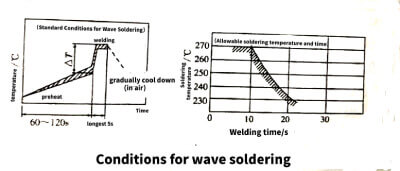
💐When components are immersed in solder after mounting, it is important to maintain the temperature difference between the components and the solder within the recommended range for the components being soldered. Do not wave solder components that are not stated to be wave solderable. However, it should also be noted that, in the case of repeated welding, the cumulative welding time shall not exceed the welding time shown in Figure 3.53.
🌷Too thick solder paste used in wave soldering will result in too much solder, which will make the chips on the PCB more susceptible to the mechanical and thermal stress of the circuit board, and may cause chip damage. Too little solder paste will cause insufficient bonding strength on the external electrodes, resulting in the chip falling off the PCB. The optimum solder volume for wave soldering is shown in Figure 3.54.

3.6 Use a soldering iron for correction or hand soldering
🌈When calibrating or hand-soldering individual components, a soldering iron is required, and the following points need to be paid attention to in this soldering environment.
🦙The sudden temperature rise of the multilayer ceramic capacitors will cause deformation due to the internal high temperature difference, which will damage the chip. Therefore, during preheating, please maintain the temperature difference ΔT within the recommended range for the components to be soldered. Of course, the smaller the ΔT value, the smaller the pressure on the chip. It should be noted that the soldering times/temperatures given in Figure 3.55 are cumulative soldering (including reflow and wave soldering) times/temperatures.
🐐Standard heating conditions and allowable times for this type of welding are within the ranges shown in Figure 3.55.
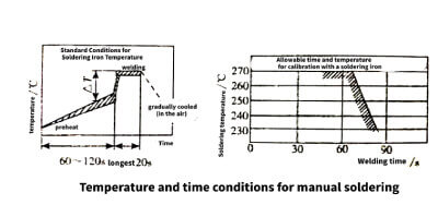
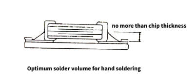
🦌Note when using a soldering iron for calibration or soldering: the optimal amount of solder paste/solder does not exceed the chip thickness, as shown in Figure 3.56. The soldering iron should be limited to 20W, the components should be preheated to 130°C, the temperature of the soldering iron tip should not exceed 300°C, the diameter of the soldering iron tip should not exceed 3mm, and the longest soldering time should be 5S. Do not let the soldering iron tip directly touch the ceramic capacitor components. itself etc. If soldering 1mm from the root of the ceramic capacitor terminal, be careful not to let the tip of the soldering iron touch the capacitor directly. But there is no need to preheat, it is best to complete the soldering with the soldering iron tip within 3S when the working temperature is lower than 270℃.
🐕Similar to wave soldering, manual soldering also requires attention to the amount of solder. The optimum soldering amount for manual soldering is shown in Figure 3.56, that is, the solder should not exceed the height of the component.
4 Effects of PCB Design on Soldered and Mounted Components
The design of the PCB also directly affects the quality of the multilayer ceramic capacitors after installation. Therefore, the following matters should be paid attention to when designing the PCB.
4.1 Precautions for PCB layout
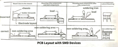
🐾Unlike lead components, chip components are susceptible to bending stress because they are mounted directly on the substrate. And they are more sensitive to mechanical and thermal stress than leaded components. Too much solder can increase these stresses, which can lead to chip breakage. Therefore, when designing the substrate, the pad layout and size should be considered to avoid excessive soldering. Figure 3.57 shows the PCB layout with SMD components.
🌲The common error in the layout of all the incorrect PCB components in the picture is due to the fact that there are other solder joints near the multilayer ceramic capacitors and there is no solder mask between the pads, resulting in too much solder for the multilayer ceramic capacitors and increasing the number of laminations
The stress of ceramic capacitors can cause damage to multilayer ceramic capacitors. The solution is to have non-welded areas between components to avoid excess solder.
4.2 Pad size of multilayer ceramic capacitors
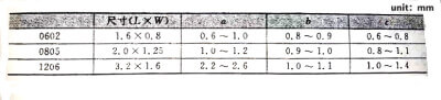
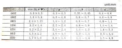
🦔The pad size of the multilayer ceramic capacitors also directly affects the welding quality. The pad size of different welding processes is slightly different. The specific size of the pad of the multilayer ceramic capacitors is shown in Figure 3.58.
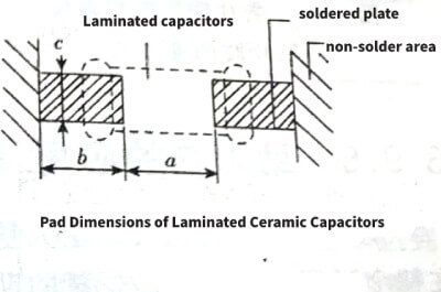
🍀The specific dimensions of the pads of the wave-soldered multilayer ceramic capacitors are shown in Table 3.13. Pads for Reflowed multilayer ceramic capacitors
🌱The specific dimensions are shown in Table 3.14.
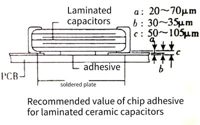
5 Correct application of adhesives
🌹Too thin or insufficient adhesive will cause the chip to loosen or fall off during wave soldering. The amount of adhesive should be larger than the dimension C in the dimension shown in Figure 3.59 to achieve sufficient bonding strength. The electrode thickness and pad thickness of the chip must also be taken into account. Low-viscosity adhesives will cause the chip to slip after placement, and the adhesive must have a viscosity of at least 5000Pa.s (500ps) (at 25°C). Adhesive dosage: 0603/min. 0.05mg, 0805/min. 0.1mg, 1206/min. 0.15mg.
🌺Adhesive curing: Insufficient curing of the adhesive will cause the chip to fall off during wave soldering, and the insulation resistance between the external electrodes will decrease due to moisture absorption. It is necessary to control the curing temperature and time to avoid insufficient curing.
6 Application of flux
🌸Too much flux will generate a lot of gas, resulting in reduced solderability. Therefore, a small amount of flux should be used evenly throughout the process (foaming systems are generally used for wave soldering). Too high a halide content in the flux may cause corrosion of the external electrodes unless adequate cleaning is performed. If a flux with a halide content of up to 0.2wt% is used, then a thorough cleaning is required: if not cleaned sufficiently, the water-soluble flux can cause a decrease in the insulation resistance between the external electrodes. Care must be taken not to use strongly acidic fluxes.
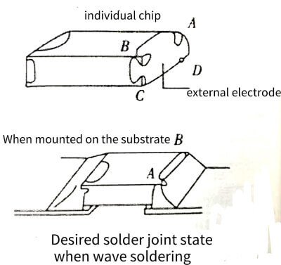
7 Wave Soldering
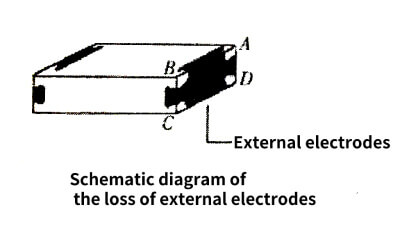
⛄️Pay attention to the temperature and time to ensure that the external electrodes are not leached by solder more than 25% of the terminal area of a single chip (that is, the full length of the ABCD surface as shown in Figure 3.60), and 25% of the AB length when mounted on the substrate , as shown in Figure 3.60.
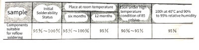
(1)🍹Test method: Put the chip capacitor under the following conditions, then apply flux (25% rosin in ethanol solution) to the chip, and then immerse it in mixed solder at 230°C for 2s.Conditions: exposed at room temperature (6 months and 12 months respectively), placed under high temperature conditions (100h at 85°C), placed under humid conditions (90% to 95% relative humidity at 40°C) 100h).
(2)Test samples: products suitable for wave/reflow soldering.
(3)🍸Acceptance criteria: Measure the surface area of the external electrodes covering the mixed solder using a 60x optical microscope.
(4) The test results are shown in Table 3.15.
8 PCB solder volume and bending strength
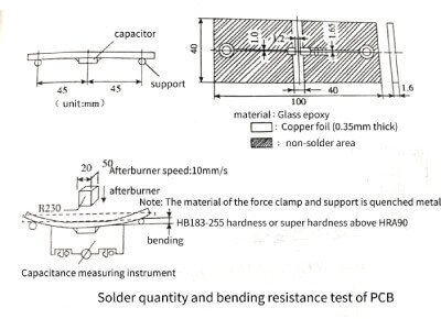
(1)🪀Test method: Solder the chip capacitor on the test PCB. The amount of solder paste is subject to the thickness of the chip. Then bend the PCB as shown in Figure 3.61 and test the electrostatic capacity.
Matters-needing-attention-in-the-storage-and-use-of-laminated-ceramic-capacitors.jpg)
(2) Test samples: products suitable for wave/reflow soldering. Component thickness T=0.6mm (T=0.6mm is mentioned later to uniformly weld the thickness of the component). (3) Acceptance criteria: If the change in electrostatic capacity exceeds the value specified in Table 3.16, it should be regarded as a defective product. (4) Test results: The test results are shown in Figure 3.62.
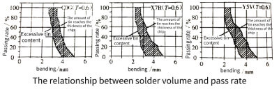
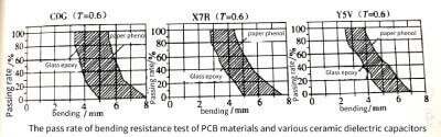
🌿For glass epoxy substrates, the pass rate of the welded multilayer ceramic capacitors is 100% when the bending is within 2mm. The performance of X7R is relatively the best, X7R is relatively second, and Y5V is relatively the worst.
🌔When the soldering amount reaches the thickness of the component, the CoG dielectric capacitor can withstand about 3.3mm, the X7R can withstand about 2.7mm, and the Y5V can withstand about 2.5mm, and the components can reach 100% pass rate. When the amount of solder is too large, the bending that can pass 100% will decrease. At the same time, no matter what the conditions, excessive bending will cause the pass rate of the multilayer ceramic capacitors after welding to decrease.
9 Solder Amount and Temperature Cycling
(1) Test method: Use solder to solder the chip on various test fixtures of the substrate, and the amount of solder is subject to the required thickness of solder. The clamps were then cycled 200 times through the temperature shown in the top panel of Figure 3.63.
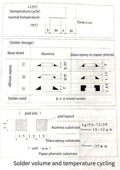
🐚Alumina substrates are typically used for reflow soldering, while glass epoxy or paper phenolic substrates are typically used for wave soldering, as shown in the middle panel of Figure 3.63. The material thickness is 0.64mm alumina, 1.6mm glass epoxy resin, and 1.6mm paper phenol. The above solder dosages are indicated by ①, ②, and ③ respectively in Figure 3.64. The pad dimensions are shown in the bottom image of Figure 3.63.
(2) Test sample: capacitor dielectric C0G/X7R/Y5V dielectric, thickness T=0.6mm.
(3) Acceptance criteria: If the change of electrostatic capacity exceeds the following specified value, it should be designated as a disabled product. Characteristics Capacitance change: COG within ±2.5% or ±0.25pF (whichever is greater): X7R within ±7.5%; Y5V within ±20%.
(4) The test results are shown in Figure 3.64.
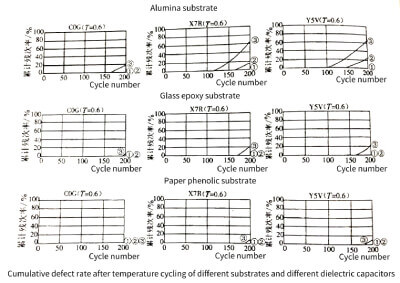
🍌It can be seen from 3.64 that the substrate of any material can withstand more temperature cycles when the solder height is equal to the component height. The solder group with the same height as the component has passed the test of 200 thermal cycles. When the aluminum substrate is soldered at 1.6 times the height of the component, the defect rate begins to occur after more than 100 times. It can be seen that the height of the solder is the most important factor affecting the thermal cycling test of the multilayer ceramic capacitors.
🥧Among the three mediums, C0G has the best thermal cycle resistance, X7R is the second, and Y5V is relatively the worst. Different material substrates also have a great impact on the thermal cycle performance of the assembly, with the aluminum substrate being the largest, probably because the expansion coefficient of aluminum is the largest here. The glass epoxy substrate is better, while the paper phenol substrate, which is not very good in other properties, is relatively the best. The possible reason is that the paper phenol substrate is relatively soft.
10 Flexural strength of PCB materials
(1)💥Test method: Solder the chip on the test board, as shown in Figure 3.65. Then bend the test plate as shown in Figure 3.66, and measure the electrostatic capacity.🦋
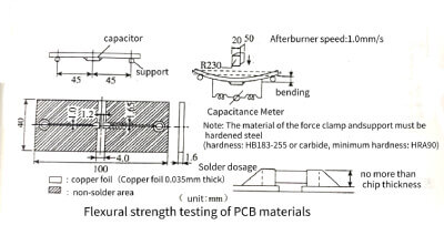
(2)Test sample: C0G/X7R/Y5V medium, the thickness of the component is T=0.6mm.
(3)🤹Acceptance criteria: If the change of electrostatic capacitance exceeds the following specified value, it should be regarded as defective product. Characteristic Capacitance Change: C0G is within ±5% or ±0.5PF (whichever is greater); X7R is within ±12.5%; Y5V is within ±20%.
(4) The test results are shown in Figure 3.66.
🍖Among the three kinds of media, the C0G medium has the best bending resistance, and still has a 100% pass rate when the substrate is bent by 3mm, and Y5V is the worst. The glass epoxy resin substrate has a worse effect on the flexural performance of the ceramic capacitor than the paper phenol substrate, and the substrate bending is about 1.5mm worse.
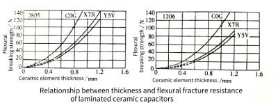
11 Fracture strength of multilayer ceramic capacitors
(1)🐻Test method: Place the chip on the steel plate shown in Figure 3.67. Increase the load near the center of the test sample.
(2) Test sample: Anti-fracture characteristics of 1206/0805 packaged G0G/X7R/Y5V dielectric capacitors.

(3)🐼Acceptance criteria: The amount of load that causes chip breakage or cracking can be defined as bending force.
(4) Explanation: The fracture strength P is proportional to the square of the thickness of the ceramic component, which can be represented by a quadratic curve:

Among them, W, T, L, y are the width (mm) of the ceramic component, the thickness of the component (mm), the distance between the fulcrums (mm) and the bending stress (N/m).
(5)🐹Test results: as shown in Figure 3.68.
12 Thermal Shaking
(1)🦄Test method: After applying flux (25% rosin in ethanol solution), immerse the chip in a solder bath (6X4 mixed solder) according to the following conditions, as shown in Figure 3.69.

(2) Test sample: C0G/X7R/Y5V dielectric multilayer ceramic capacitors in 0805 package, thickness T=0.6mm
(3)🐰Acceptance criteria: Use a 60x optical microscope to visually inspect the test samples, and chips with cracks or cracks should be rated as defective.
(4) Test results: as shown in Figure 3.70.
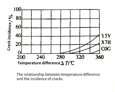
🍔It can be seen that all dielectric types of ceramic capacitors with a temperature difference below 275 °C have no cracks. The temperature difference is less than about 290 ℃, and the X7R has no cracking phenomenon. Even if the temperature difference reaches 320 °C, there is no cracking phenomenon in CoG. From this point of view, when manually calibrating or soldering, either preheat the device or limit the temperature of the soldering iron to at least 300°C.
13 Solder heat resistance
(1)🌝The test method is as follows.
①Reflow soldering: Apply 300um solder paste on the alumina substrate. After reflow soldering, take out the chip to check whether the external electrode has been leached by solder.
②Wave soldering: After immersing the test sample in the flux tin (mixed solder) with tweezers, check whether the external power has been leached by the solder.
(2) Test sample: multilayer ceramic capacitors in 0805 package, thickness T=0.6mm for wave/reflow soldering.
(3) Acceptance criteria: The start time of leaching should be defined as the loss of the outer electrode as shown in Figure 3.71 ABCD faces 25% of the total time length.
After immersing the test sample in static tin (mixed solder) with tweezers, check whether the external electrode has been leached by solder. The flux used was 25% rosin in ethanol.
(4) Test results: as shown in Figure 3.72
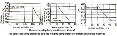
🍥It can be seen that the leaching start time of reflow soldering is the longest, about 180S. The initial leaching time of wave soldering is the shortest, about 12-13S, while dip soldering takes about 22S. In the actual welding process, corresponding to different welding methods, the welding time should be limited to the above time.
14 Thermal oscillations during calibration with a soldering iron
(1)🦟Test method: Use a soldering iron and solder wire that meet the following conditions to solder the chip welds that have been soldered on the paper phenol substrate, as shown in Figure 3.73 (Note: The soldering iron tip should not directly touch the ceramic components of the chip).
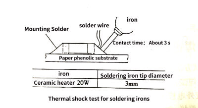
(2)Test sample: 0805 packaged multilayer ceramic capacitors COG/X7R/Y5V dielectric, thickness T=0.6mm.
(3)🦒Acceptance Criteria: Visually inspect the appearance of the test samples using a 60x optical microscope, and any samples with cracks or cracks should be rated as defective.
(4) Test results: as shown in Figure 3.74.
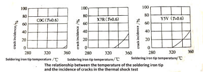
🍬It can be seen that cracks start to occur above 320°C. For paper phenol substrates, the soldering iron tip is generally allowed to have a higher temperature. In fact, the heat resistance of paper phenol substrates is not as good as that of glass epoxy resin substrates.
15 Problems that need to be paid attention to when cleaning
🌯Precautions for cleaning printed circuit boards
(1) After installing all capacitors, when cleaning the printed circuit board, it should be selected according to the flux used and the purpose of cleaning (such as to remove the residual flux during soldering or other materials in the production process). Appropriate cleaning solvent.
(2) The cleaning conditions should be checked and confirmed that the cleaning process does not affect the characteristics of the capacitor.
🍫The main points of printed circuit board cleaning:
(1) If an inappropriate solvent is used, other substances such as flux residues will stick to the capacitor or damage the outer coating of the capacitor, resulting in a decrease in the electrical properties (especially insulation resistance) of the capacitor.
(2)🌺Improper cleaning conditions, insufficient cleaning, and excessive cleaning may cause damage to capacitor performance. Under the condition of ultrasonic cleaning, excessive power output may cause excessive vibration of the printed circuit board to break the capacitor body and the welded part, or reduce the strength of the terminal electrode. Therefore, please carefully consider the following conditions: the ultrasonic output is below 20W; the ultrasonic frequency is below 40kHz; the ultrasonic cleaning time is below 5min.
(3) If the ultrasonic oscillation frequency is too high during cleaning, it may cause the PCB to resonate. As a result, the chip is damaged or the solder joint is cracked. Care should be taken not to vibrate to the PCB.