1.Snubber Capacitors as MOSFET and IGBT Switches
To transfer the stress impact experienced by MOSFET and IGBT switches during the turn-off process, especially to limit the induced potential generated by parasitic inductance during turn-off, capacitors are often needed as snubber elements. XUANSN’s IGBT snubber film capacitor are a core adaptable component. The principle of capacitor snubber circuits has been discussed in many documents and will not be repeated here. This section only describes the required performance and usage precautions for snubber capacitors used in MOSFET and IGBT switches.
Common IGBT snubber circuits mainly come in three forms, as shown in Figure 1. The bus voltage snubber circuit is shown in Figure 1(a), and its greatest advantage is its simplicity. A single low-inductance buffer capacitor is directly connected to the DC bus of the IGBT inverter to form a bus voltage buffer circuit. This type of buffer circuit only suppresses voltage spikes caused by the parasitic inductance of the DC bus and does not transfer the switching stress of the IGBT. It is suitable for small-power IGBT modules and is used for effective and low-cost control of transient voltages. Figure 1(b) shows a DC bus buffer circuit composed of an RCD, which is suitable for larger-power IGBT modules. The buffer diode D can conduct in the forward direction to allow the buffer capacitor to withstand transient voltages, and when it blocks in the reverse direction, it can allow the buffer capacitor to release excess energy through the resistor (forming an overdamped 1CR circuit), thereby suppressing parasitic oscillations that may be caused by the parasitic inductance of the DC bus. Its RC time constant should be designed to be 1/3 of the switching period, i.e., ꚍ=T/3=1/3ƒ, to ensure that excess charge on the buffer capacitor is “completely” released through the resistor. This circuit is essentially the same as the one in Figure 1(a), and therefore cannot transfer the switching stress of the IGBT. Figure 1(c) shows a snubber circuit composed of a P-type RCD and an N-type RCD, which can effectively transfer the switching stress during the IGBT turn-off process and reduce the IGBT turn-off loss. It is suitable for high-power IGBT modules and has better functionality than the snubber circuits in Figures 1(a) and (b), with a smaller loop inductance. If used in conjunction with the snubber circuit in Figure 1(a), it can further reduce the stress on the snubber diode and improve the snubber effect. Its core energy storage and voltage absorption element is still the IGBT snubber film capacitor.
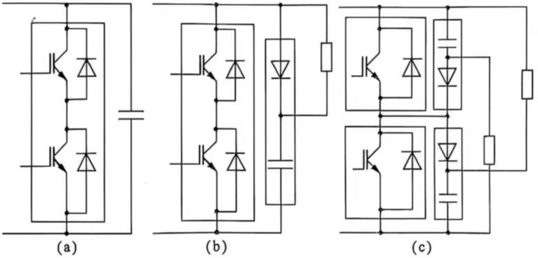
Figure 1 Snubber Circuit for IGBT Switching Circuit
To illustrate the function and selection criteria of the snubber circuit, an example is provided here. The typical turn-off voltage waveform of the IGBT after using a snubber circuit is shown in Figure 2. In the figure, the voltage spike ∆V1 at the beginning of VCE is caused by the parasitic inductance of the snubber circuit and the recovery process of the snubber diode. Its value is:
![]() (1)
(1)
Where Ls and di/dt are the parasitic inductance of the buffer circuit and the current rise rate at the moment of turn-off or diode recovery, respectively. In the worst case, the current change rate is close to 20 ic (A/μs).
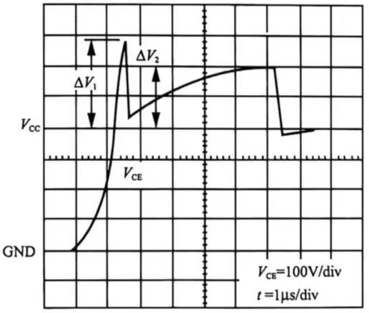
Figure 2 Voltage waveform of IGBT turn-off process using buffer circuit
If ∆V1 has been set, the maximum allowable inductance of the buffer circuit can be determined by equation (1). For example, if the maximum operating current of an IGBT circuit is 400A and ∆V1≤300V, then in the worst case:
![]() (2)
(2)
From equation (1), we get
![]() (3)
(3)
That is to say, under this condition, only parasitic inductance below 37.5nH is allowed in the circuit. Usually, the parasitic inductance of the buffer capacitor itself is about 20nH. In Figure 2, ∆V2 is the peak value of the current voltage as the buffer capacitor charges. It is related to the value of the buffer capacitor and the parasitic inductance of the bus, and can be determined using the law of conservation of energy. As mentioned earlier, the energy stored in the bus inductance and the stray inductance inside the buffer circuit and its components during IGBT turn-on is transferred to the IGBT snubber film capacitor. Therefore, we have:
![]() (4)
(4)
Where Lp is the parasitic inductance of the bus; I is the operating current; C is the value of the buffer capacitor; and ∆V2 is the peak value of the buffer voltage. Similarly。
if ∆V2 is already set, the value of the buffer capacitor can be determined by equation (4).
It is easy to see from equations (1) and (4) that high-power IGBT circuits require the bus inductance and the stray inductance inside the buffer circuit and its components to be as small as possible. This not only reduces ∆V1 but also reduces the value of the buffer capacitor, thereby reducing costs.
Table 1 provides recommended values for buffer capacitors for different DC bus inductances and IGBT module capacities, as provided by CDE capacitor distributors and XUANSN. This table is calculated using equation (4) when ∆V2 ≤ 100V.
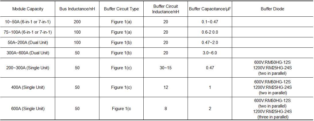
Table 1 Recommended Values for Buffer Capacitors
An empirical estimation method is to typically use approximately 1 μF of buffer capacitor per 100A collector current. This value effectively suppresses transient voltages.
Bus inductance and stray inductance within the snubber circuit and its components have a significant impact on IGBT circuits, especially high-power IGBT circuits. Therefore, it is desirable for them to be as small as possible. The low inductance characteristic of the IGBT snubber film capacitor itself is crucial. To further reduce the overall inductance, multiple approaches are needed.
First, the DC bus should be as short as possible.
Second, the buffer circuit should be placed as close to the module as possible.
Third, low-inductance polypropylene non-polar capacitors, fast-speed buffer diodes matched to the IGBT, and non-inductive discharge resistors should be selected.
Fourth, other effective measures.
Currently, there are various manufacturing processes for buffer circuits: some use discrete components; some use printed circuit boards; and some directly mount the buffer capacitor module onto the IGBT module. Clearly, the last method, because it meets the second and third measures mentioned above for reducing parasitic inductance, is the most effective. The buffering effect is the best, maximizing the protection of IGBT safe operation. Therefore, IGBT buffer capacitors are often packaged/mounted in a way that allows direct mounting to the leads of the IGBT module, as shown in Figures 3-5.
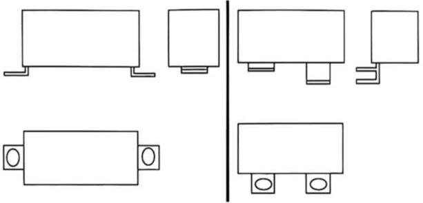
Figure 3 Package of DC bus type buffer capacitor
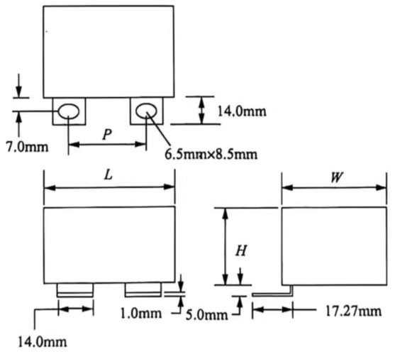
Figure 4 DC bus type buffer capacitor
The DC bus type buffer capacitor modules shown in Figures 3 and 4 are suitable for applications with relatively low-power IGBT inverters. They can also be combined with external diodes and resistors to form a module suitable for higher-power IGBT inverters. The advantage of this packaged module form is that its mounting dimensions are perfectly suited for six-unit and seven-unit IGBTs. The positive and negative power terminals of the module are the same size, making installation extremely convenient. For example, CDE’s SCD type, EP-COS’s MKP series, and XUANSN’s dedicated modules are all single-unit packages, forming the structure shown in Figure 3 or Figure 4. This type of IGBT snubber film capacitor module forms a buffer circuit suitable for IGBT modules with medium to small current capacities, absorbing transient voltages from high DC power buses. Capacitance ranges from 0.22 to 4.7 μF, with five DC voltage levels: 600V, 1000V, 1200V, 1600V, and 2000V. Its characteristics include low dielectric loss, low inductance (<20 nH), self-healing capability, and fire-resistant resin encapsulation for direct mounting on the IGBT module.
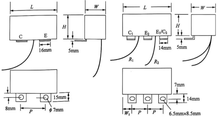
Figure 5 RCD type IGBT buffer circuit module outline and dimensions
Figure 5 shows the RCD type buffer capacitor module, such as CDE’s SCM RCD type and SCC type capacitor modules are available. The RCD type is a single-unit buffer capacitor and buffer diode package, as shown in Figure 5. Similar to the DC bus type buffer capacitor, the RCD type buffer capacitor module can also be directly connected to the IGBT electrode via bolts. To simplify the structure and reduce parasitic inductance, the diode is directly packaged with the buffer capacitor within the same module [see Figures 3(b) and (c)]. Specific installation dimensions can be found on the manufacturer’s website. The RCD buffer capacitor module and external resistor constitute the buffer circuit shown in Figure 3. It is suitable for IGBT modules with medium and small current capacities. Depending on the location of the buffer capacitor, there are P-type and N-type: P-type modules have the buffer capacitor connected to the positive DC power bus (P bus), while N-type modules have the buffer capacitor connected to the negative DC power bus (N bus). N-type capacitor modules are suitable for one or two units. IGBT modules. If two single-unit IGBT modules are connected in series and the buffer circuit shown in Figure 3(c) is used, the P-type IGBT module is connected in parallel to the P bus terminal, and the N-type IGBT module is connected in parallel to the N bus terminal. Capacity range: 0.47~2.0μF, DC voltage: 600V and 1200V. Features include low dielectric loss, low inductance, integrated package of buffer capacitor and fast reverse recovery diode, wire connection to external resistor, fire-resistant resin encapsulation, and direct mounting on the IGBT module; the SCC type capacitor module consists of a two-unit buffer capacitor and buffer diode package, forming the buffer circuit shown in Figure 3(c) with an external resistor. Suitable for high-current capacity two-unit IGBT modules. Capacity: 0.47~2.0μF, DC voltage: 600V and 1200V. Features include low dielectric loss, low inductance, high peak current, integrated package of buffer capacitor and ultra-fast recovery diode, wire connection to external resistor, fire-resistant resin encapsulation, and direct mounting on the IGBT module. On the module.
The selection criteria for buffer capacitors or pulse capacitors used in other buffer circuits or fast charge/discharge circuits are the same as those for IGBT buffer capacitors.
2.As high-frequency rectification and filtering capacitors
The biggest advantage of film capacitors is that their ESR can be minimized, and they can withstand larger peak currents and RMS currents, making them ideal for high-frequency rectification and filtering applications. Especially at voltage levels that aluminum polymer electrolytic capacitors, tantalum/tantalum polymer electrolytic capacitors, and high-capacitance ceramic capacitors cannot reach, XUANSN’s IGBT snubber film capacitor exhibit excellent performance.
High-frequency rectification and filtering requires capacitors to have the lowest possible parasitic inductance and ESR. Film capacitors for switching power supplies, such as CDE’s 935 type capacitor, can achieve ESR and ripple current of 6mΩ/30A/400V/10μF, 6mΩ/27.4A/200V/20μF, and 6mΩ/24.3A/100V/30μF, respectively, with AC RMS values of 30A, 27.4A, and… At 24.3A, the corresponding peak ripple voltages are approximately 510mV, 465mV, and 413mV, which is very small for output voltages above 100V. CE’s 30V/80μF capacitor has almost zero ESR, and its external leads are copper plates. The 75V/40μF capacitor uses 13 standard DIP pins per lead to minimize ESR. Furthermore, the ESR of the IGBT snubber film capacitor used for high-frequency rectification and filtering directly affects the peak value of the output voltage ripple.