Previously, we discussed the charging characteristics of a capacitors in an RC circuit. In this section, we will examine the discharge characteristics of the capacitor. The corresponding simulation circuit and parameters are shown in Figure 1.1.
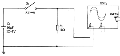
Figure 1.1 Simulation circuit and parameters for capacitor discharge characteristics
Note: In the simulation circuit, the initial voltage (Initial Condition, IC) across capacitor C1 is not 0V. When switch S1 is closed, the energy stored in capacitor C1 discharges through resistor R1, and the waveform across the resistor is shown in Figure 1.2.
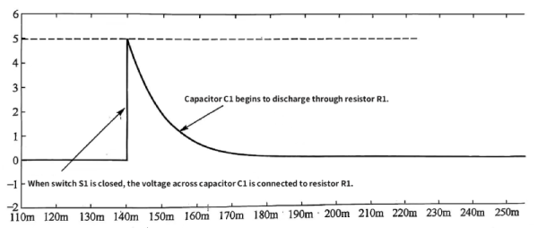
Figure 1.2 Waveforms at the resistor terminals
Does this look familiar? It’s the same as the output waveform of an RC differentiator circuit (the waveform across the resistor).
We analyze the monostable trigger circuit shown in Figure 1.3.. Its output pulse width is determined by the discharge time constant of the capacitor.
As shown in Figure 1.3, this monostable multivibrator circuit consists of a NAND gate, a NOT gate, a resistor, and a capacitor. As long as the input VIN has a sufficiently wide positive pulse, the output VOUT will generate a timed pulse with a width of tw, which is determined by the time constant. The input and output waveforms are shown in Figure 1.4.
Before time t0 (in the idle state), the input trigger signal VIN is at a low level. The output potential VA of the NOT gate is therefore at a high level. This charges capacitor C1 through resistor R1. The potential VB is the same high level as VA. One input of the NAND gate receives the low level from VIN, so the output VOUT is at a high level. At this point, the circuit is in its initial stable state, as shown in Figure 1.5.
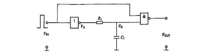
Figure 1.3 Monostable trigger circuit
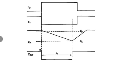
Figure 1.4 Input and output waveforms
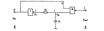
Figure 1.5 Initial stable state of the circuit
When time t0 arrives, the input VIN flips to a high level, and the output VA of the NOT gate becomes a low level (1 becomes 0), which is equivalent to being grounded. Capacitor C1, having already been charged, discharges through resistor R1. As long as the potential VB is greater than VIL (the low-level threshold voltage of the NAND gate input), the output state will remain at a low level, as shown in Figure 1.6.
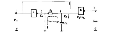
Figure 1.6 Timed capacitors discharge
During the discharge of capacitor C1, if the input VIN is switched to a low level, the output of the NAND gate will immediately switch to a high level, indicating that the input affects the state of the circuit. Therefore, the positive pulse width of the input must be longer than the timing pulse width, which is different from other monostable multivibrator circuits.
When the continuous discharge of capacitor C1 causes the VB potential to be less than VIL (the NAND gate considers the input to be low), the output becomes high, returning to a stable state. At this point, the input positive pulse can be removed, as shown in Figure 1.7.
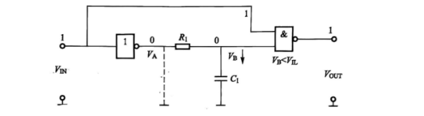
Figure 1.7 Circuit returning to a stable state.
We will perform a simulation using the circuit parameters shown in Figure 1.8.
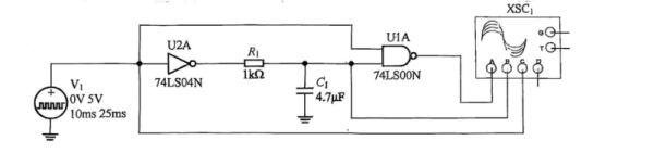
Figure 1.8 Simulation circuit
The corresponding input and output waveforms are shown in Figure 1.9.
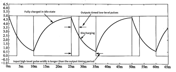
Figure 1.9 Related input and output waveforms
Some applications require the capacitor’s discharge time constant to be as large as possible (ideually, no discharge at all), such as in peak detector circuits. The function of a peak detector is to extract the peak value of the input (analog) signal V1, producing an output voltage Vo = V1(PEAK), as shown in Figure 1.10.
Ideally, the output voltage Vo of the peak detector circuit should be the maximum value of the input signal V1, and should remain at the current maximum peak value when the input signal is below the maximum peak, until a larger peak appears.
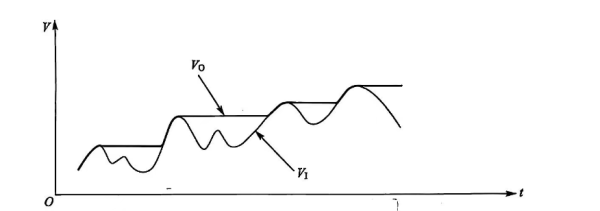
Figure 1.10 Output tracks the input peak.
Peak detection circuits are widely used in measuring instruments, such as in automatic gain control (AGC) and for obtaining the maximum value from sensors. Their basic structure is shown in Figure 1.11.
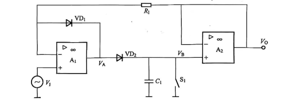
Figure 1.11 Basic structure of a peak detection circuit
In this circuit, capacitor C1 serves as the peak value storage unit for the input analog signal; diodes VD1 and VD2 are unidirectional current control devices, allowing unidirectional charging of the capacitor only when a peak occurs; A1 and A2 are both connected as voltage followers for isolation; additionally, there is a capacitor discharge reset switch S1 (usually a FET), which can be used to initiate a new peak acquisition cycle, although this switch is not essential.
When a new input peak V1(PEAK) arrives, the output VA of A1 is positive, at which point VD1 is off and VD2 is on. A1 is in a deep negative feedback state through the path of VD2, A2, and R1, so the potential at the inverting input of A1 follows the potential at the non-inverting input (virtual short characteristic). That is, the circuit output VO tracks the input signal V1 in real time (tracking mode). At this time, the output current of A1 charges capacitors C1 through VD2, and the output voltage VA of A1 is higher than the output voltage VO of A2 by a transistor voltage drop, i.e., VA = VO + VVD2, as shown in Figure 1.12.
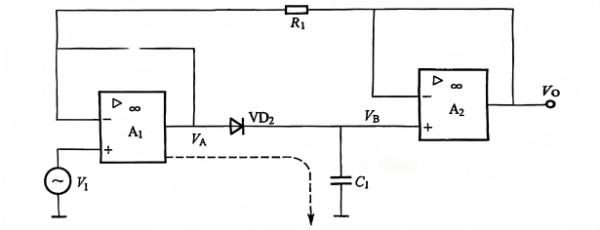
Figure 1.12 Circuit state after the arrival of a new peak.
When the input V1 begins to decrease, the output VA also decreases. Since VA is less than VB (C1 stores the most recent peak value), the diode VD2 is reverse-biased. At this point, capacitors C1 has no discharge path, and the circuit enters a hold mode. VO remains at the previous peak voltage (VB), and diode VD1 is forward-biased, as shown in Figure 1.13.
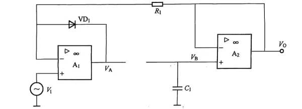
Figure 1.13 Circuit state after the peak
To ensure the charging speed and accuracy of capacitors C1, A1 should be an operational amplifier with a strong load driving capability (large output current) and low DC input error. A2 requires a sufficiently low input bias current so that the discharge of capacitors C1 during the hold mode is minimal. Additionally, VD1 and R1 are used to prevent A1 from saturating after detecting the peak, thus avoiding affecting the circuit’s response speed when a new input peak appears.
This article provides an in-depth analysis of the discharge characteristics of capacitors and their applications. The article uses simulated waveforms to explain the time constant, pulse width formation mechanism, and peak holding principle.For more information on capacitors, please visit: www.xuanxcapacitors.com